Another week has gone by already? Well, I do at least have something to show for it.
So the thing I spent the most spare time on this last week has been designing a FPGA-based PCI card. This is something I’ve wanted to do for some time now (and have an earlier unfinished attempt that was far more complex), but I have recently encountered some inspiration for a board that will be somewhat useful, or at least interesting.
This board isn’t really much of anything special, but it will fill a specific niche, and will be sufficient to try out a lot of interesting things I’ve been thinking of in the PCI space.
So, This isn’t going to be an exceptionally impressive post, but I did collect screenshots from various stages of the board’s development, and I’ll also discuss the design decisions behind this board.
On with the screenshots!
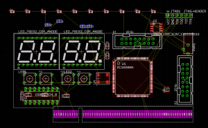
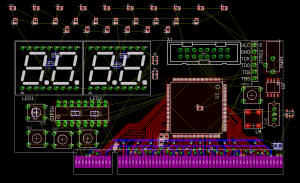
(Just getting started, have finished the core of the schematic, have all the power and parts set up)
(After working out the pin mappings from FPGA to PCI card, adding some PCI-related capacitors)
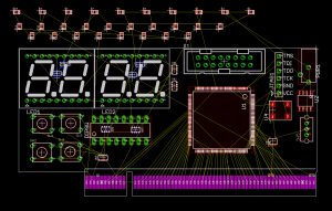
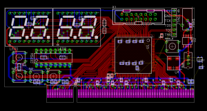
(Fixed the PCI – fpga mappings slightly and started routing. This is a few hours of progress, but it takes a lot of effort…)
(Continuing to route PCI-FPGA traces)
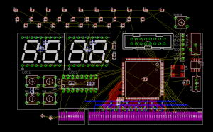
(Ah. Done with that. A few things move around to pack better)
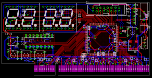
(A lot of other stuff gets routed! It’s not as hard as the PCI stuff :)
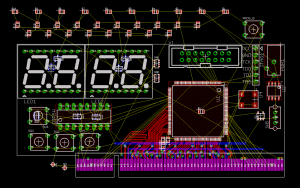
And the final part done: Routing the power pins on the FPGA. (And a few pesky remaining traces due to an error)
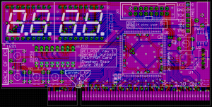
The signals on the board are now 100% routed, but the board is still not complete, I have a number of cosmetic things to do still, moving component text around and adding some descriptive text. Also planning to add ground fills to unused board space.
So, some of you may have guessed my inspiration for this board, it’s pretty similar to those “BIOS POST code display” boards – Yup, and that is one of the intended uses of this board, but by no means all it can do. This board has been designed so it can also easily work as a standalone development board for general purpose FPGA experimentation, and it is also my intention to build a full PCI Device using this board as well. Of course it’s not going to do much with this board alone, but the I/O header should allow for some interesting external devices if I want to try anything specific.
Some more specific details of the design:
- The PCB is routed with 8 mil traces (and 8 mil spacing) – this makes it pretty challenging to route, but it was fun.
- If operating only as a PCI card, it would be possible to remove several components (the power supply stuff and clock on the right side of the board), without affecting anything
- The FPGA in this case is a Spartan-3AN (XC3S50AN – not incredibly big but will work here) – the 3AN series, as opposed to most other Spartan-3 FPGAs, have onboard flash memory to store configuration data (otherwise an external chip would be needed to configure from, eating up more I/O pins)
- There are 4 I/O pushbutton switches, and an 8-switch dipswitch
- The PRSNT1# and PRSNT2# lines on the PCI connector are used to indicate to the system board whether or not a PCI card is present in a given slot. This board has solder-bridge jumpers potentially connecting those to ground (to indicate presence); In the case of a BIOS POST card we don’t actually want to indicate to the system that there is a board present, as we can get what we want without being a “full” pci device. But bridging those jumpers will also allow a full PCI device to be designed.
- The PCI connector has been routed by flipping back-side signals to the top side, and trying to align the PCI signals to the FPGA pins before even starting that; On the back side, I have a thick 3.3V trace running along the length of the connector, and a GND trace above that, which makes it relatively easy to keep all the power lines connected properly. This is the fourth or so revision of my process for doing this, and it’s pretty effective – but I noticed yet another optimization… If I also were to match up the FPGA 3.3V pins with the front-side PCI 3.3V pins, it would further reduce the complexity of routing the connector, and I’d get better connected power pins as well – Something to consider for next time, the time that goes into planning and routing the PCI connector to a FPGA is pretty significant.
I am planning to finish up the design work and get some of these boards produced in the next few days – and when I get them back and get some stuff working on them, I’ll post again on how it went, how PCI works, and other sorts of interesting things :)
Update: After a little bit more effort, I have deemed the board “complete”. Now working on getting it fabricated…
RSS feed for comments on this post. | TrackBack URI
June 14th, 2010 at 3:22 am
Are you delaying the PCI signals inside the FPGA to compensate for the differing trace lengths from PCI slot to FPGA?
June 14th, 2010 at 10:50 am
I’m not planning to delay the signals; PCI is designed to work without all of the data traces being similar in length (I suspect they understand that to make PCI devices cheaply, it isn’t necessarily always possible).
The PCI specification imposes limits on signal trace length (<1.5 inches) while also specifying that the PCI clock trace be exactly 2.5 inches long.
Given these requirements, the effects of signal skew have been controlled, so it shouldn't be necessary to delay signals internally to make a working device.
July 4th, 2010 at 12:02 am
[...] the PCI card from a few weeks [...]
August 13th, 2010 at 3:52 pm
This looks really cool. But how are you supposed to see the displays from inside the computer? You have an open box?
August 22nd, 2010 at 1:35 pm
See the followup blog post for more pictures, but if you have a motherboard on a desk in the open, it’s reasonably easy to see. However, this was designed to work with an external display too – the connector on the top of this board can connect via ribbon cable to another board which has LED displays and buttons; you can mount that outside the case somewhere you can see it.
March 18th, 2012 at 1:23 pm
Hi! Where can I get the schematic of this project?
Best regards!