Generic USB JTAG/etc Programmer
Despite having 2 weeks for this, I haven’t actually completed anything notable; So I’m just going to post some WIP images of a PCB I’ve designed to do general purpose programming (Generally jtag, but also AVR)
I’ve been working out the concepts in software using the modified USB stick (as I mentioned previously) but just haven’t had enough time to allocate to it yet. Soon, though.
This design is pretty simple; I have the microcontroller (ATMega32U2), a RGB LED, switch, and crystal – Then around that I am building a set of voltage level translation circuits for the jtag signals, and for additional inputs, outputs, and “pump” signals (which can strongly connect to a target’s V+ level, and drive a significant amount of current)
I’m including the JTAG interfaces I use commonly on the board, and I have another additional “expansion” slot which I’ll be building new boards for to connect to yet other interfaces
Schematic done, decided on a rough layout and started placing parts.
I got the core signals routed, and routed the level shifted jtag signals around the board, connecting to the side connectors as they go.
Added most of the other level shifting signals
And now the design is essentially complete!
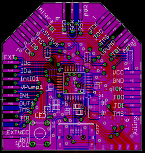
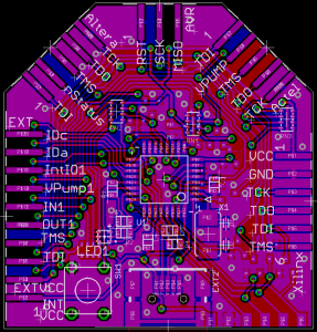
Added ground planes, and vias to keep them well connected / allow plenty of return paths.
At this point I thought I was done…. Only, oops, I connected the top 3 headers backwards; I had gone off of the pinout of the socket they plug into. Fortunately I noticed this before trying to produce the board :)
Ahh, now they’re correct.
So I’m having this board produced pretty soon and will write up more on JTAG once I have done some stuff with this.
In other news I’m taking a vacation in about 2 weeks! No, I’m not going anywhere interesting, just visiting family, but perhaps I’ll have something fun to write about by then :) I certainly have plenty of things I want to do!
RSS feed for comments on this post. | TrackBack URI
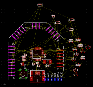
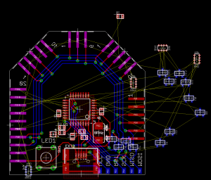
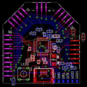
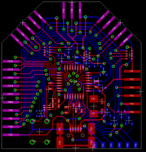
July 26th, 2010 at 2:44 am
Small comment from a homebrewer who has too little experience of PCB design …
Am I correctly understanding that your “ground plane” is an additional layer (that is, you’re not simply designing a double-sided PCB, but something more sophisticated I couldn’t replicate here) whose purpose is to avoid self-inductance on a ground-loop ?
July 26th, 2010 at 10:18 pm
Not quite; I’m just referring to a ground fill on both sides; What I’m calling attention to is that it’s not “just for show” as too many people do, you do in fact have to think about ground planes in order for them to be helpful (ground fills can in fact be detrimental to a design if they’re just thrown on without any care).
The first part of this is making good return paths. Anything that is going to use electricity needs a good path to get that electricity, and a good return path to the source of that electricity (generally through ground) – The more twisted and obscure that path is, the higher the inductance will be, so making sure your components have good return paths is important. This applies more so to ground than the voltage paths – most components can tolerate the voltage jumping around a little, but the infamous “ground bounce” can cause serious problems.
The other thing I’m doing here (which goes along with return paths) is keeping the 2 layers of the ground fill well connected – I try to via at corners of the ground plane so there isn’t any part that’s isolated by itself. My goal is to keep the ground potential as even as possible across the entire fill, otherwise noise and heavy current usage could change the potential significantly in some areas, causing problems for sensitive components or analog work.
All that being said, it doesn’t really matter much for this design :) but it’s fun to think about and design for.