The road to 3D Printing, part 3
As I mentioned earlier, JTAG is a pretty simple protocol. For the ucHelper I’ve designed a command-oriented serial protocol that allows me to perform various JTAG and UART operations. After some initial trouble with physical connections on the CNC board, it was possible to enumerate the JTAG chain! In order to be sure JTAG was really working as intended, I took a short detour and wrote an SVF player, and was able to program some existing Xilinx FPGA boards from SVF files (like serialeth).
The ARM Chip I was using on the CNC board (NXP LPC2927) has two JTAG chains – one of them is a boundary scan / flash (and who knows what else) chain, and the other is for the ARM9 standard debug interface. I only really wanted to program the flash, so I started out with the flash chain – There was some documentation for the JTAG flash interface of a previous chip in the series so I was hopeful this one would be similar.
Unfortunately it was not meant to be. The enable bits / initial handshake sequence for the flash controller on this chip seems to be entirely different than the earlier one, sometime I may go back and find the right bits to make that work, but I shifted my focus to using the ARM debug interface. The first thing I noticed, is that it didn’t work :) As it turns out (after connecting the layers of deep indirection in the documentation), you must have a crystal in a specific range of frequencies for it to work; After fixing that though, I began to make progress on that front. the ARM debug interface for this chip is relatively well documented in the ARM9 documentation on ARM’s site. Documentation always seems to leave something to be desired, but this was at least relatively unambiguous – and worked!
Effectively, the ARM9 chips (also most other ARM chips), for a debug interface, simply intercept the processor’s instruction and data busses, and allow you to single step the processor. So you can perform operations by injecting the instruction you wish to execute, and single stepping. You can write a register to an arbitrary memory location, which causes it to be intercepted on the data bus (afterwards you can read the data bus) – Similarly you can read from memory and it will end up reading the value you insert onto the data bus into a register. It’s a rather minimal and effective debugging interface, it doesn’t consume much in the way of hardware resources, though the software to do anything useful with it has to be a bit complicated as a result.
Since the single step operations capture the data bus, it’s not possible to directly modify or read system memory through them, but there is another special provision for doing this, for executing individual instructions synchronized with the normal CPU clock that can interact with memory. So, I wrote a handful of wrappers that would allow me to manipulate the CPU’s registers and read from / write to memory, and around that built a small program that wrote the flash using the system’s internal flash controller.
With that literal pile of work behind me, I set off building software for the ARM chip itself. A short amount of time later, I had a blinking LED (Because this is naturally the most important thing to do with /any/ piece of hardware)
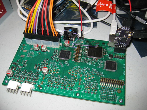
(Not visible: LEDs blinking)
(Continuity note: Note that the above board is not the same one as the board shown in part 1! At some point in messing with the JTAG chains I became sufficiently frustrated with the quality of connections on the first board, which had been reworked a few too many times perhaps, that I built a second board and took special care in making sure the JTAG chains and other important connections were in good shape. It’s a bit less than fully populated because… placing some 400-500 components is HARD!)
(More to come in part 4…)
RSS feed for comments on this post. | TrackBack URI