Project: 8×8 LED Matrix Controller
Another week has gone by, and it’s time for another project!
This week’s project is a little bit more complex than the last one, but it’s still pretty small. It’s a small board that drives an 8×8 LED matrix. It’s actually a pretty silly project because I only have a dozen or so of these LED Matrices around (I’m not sure I can even buy these specific matrices anymore) – I actually bought them back in 2005 – they’re 8×8 arrays of red/green LEDs. They’re organized with a common anode per row, and then red/green cathodes per column. (Davr also got some, and has a number of entries on his blog about his efforts)
Just for fun, I set out to design a board that would sit on the back of the LED matrix and make it easy to drive from a small microcontroller. My design goals were to have current drivers on the common anodes, and provide a shift register to easily configure the other LEDs. I also wanted to be able to easily chain multiple boards together to make a much longer array. (Read on for more details about the design…)
So, after measuring the part and setting up a part in eagle for the LED matrix, I set to work on a circuit board.
This part I actually generated a timelapse video of – you can see it here: PCB design: An LED Matrix Controller board
The video may be a little boring (perhaps I should add music or something), but my process went as follows:
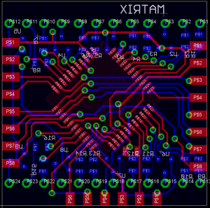
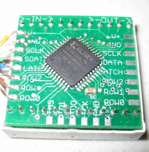
First I had to design an interface, a set of pins that would let me control the board, specifying what to display and how. I settled on a pretty simple design: There is a power and ground pin, 3 pins for selecting one of the 8 rows, and finally a serial interface into a shift register for providing the graphical data. The serial interface consists of SCLK, SDATA, and LATCH – Upon a rising edge of SCLK, the internal shift register will be advanced as the value of SDATA is pushed in. LATCH serves dual duty; a rising edge of LATCH causes the shift register’s value to be latched to the display output, and also LATCH serves as an output enable, LEDs only light up when LATCH is high.
Additionally, since I wanted this module to be chainable, I also need a second interface on the other side of the board to attach to a second board – Most of the signals are the same, but the data signal on the other side has to be an output from the shift register – just another thing to consider. I used a CPLD (the XC9572XL again!) to actually do all the intelligent work, and for switching the power to the common anodes, I used some P-FETs which are switched by the CPLD.
After getting the circuit straight, it was a bit of a challenge to actually decide what CPLD pins to use, and how exactly to lay out the board. This is always an interesting problem, and sometimes difficult, but when you keep your priorities straight it is reasonably easy to get past. In my case, power/GND and the Jtag pins dictated how certain parts of my board needed to work, and as with most cpld and fpga designs, most of the signals could have been connected to any of the pins on the CPLD. I took care to connect the serial clock pin to one of the global clock pins on the CPLD, but the majority of the pins were just connected to nearby CPLD pins for convenience. Ultimately I ended up using a 45-degree orientation for my CPLD, which I think simplified a lot of the routing.
Once the pin mappings were decided, routing was pretty simple, and didn’t take too much time; I was able to quickly route the majority of the traces, only having to move some things around for the last few traces – And that’s where the timelapse video ends. Afterwards I did wind up increasing the trace width just a bit, adding a bypass cap for the CPLD (which is important enough normally, but really important when switching power), and just cleaning some things up.
So, I submitted some PCBs to be produced via BatchPCB, and waited a few weeks for them to show up.
A few weeks pass, and they do finally show up!
It did not take long to solder one together, so the second phase of this project began: designing the CPLD code. While I designed the interface with the possibility of implementing PWM in mind (to vary the brightness of the LEDs), I opted to start with the simplest usable design first. My VHDL code which controls the CPLD performs essentially the following operations:
- Decodes the ROW0..2 to enable one of the 8 common row FETs (sets one line to low, all others to high)
- Has an internal 16bit array for the row data (8 red, 8 green LEDs). If LATCH is high, the inverse of these values will be exposed to the LEDs (as low = on), otherwise the LEDs will be off (pulled high)
- Has an internal 16bit shift register which is shifted on the rising edge of SCK (new bit is shifted in from SDATA, and the last bit is always exposed as SDATA on the other side of the board)
- When Latch transitions from low->high, the shift register is latched into the internal LED data array.
And, that’s the complete system! It is ntended to be controlled with 6 I/O pins, but you can, if you don’t mind a little bit of light bleeding, even connect SCK and Latch together and drive it with only 5 pins, which I did for testing (using an ATTiny85 chip). My ideas for improvement are a bit limited because there isn’t really much space available on this CPLD for elaborate designs… I could abandon the idea of having a separate shift register and internal display register, and use a few bits per pixel to hold a several-bit-per-pixel value, and use the LATCH signal both as a display enable and also to advance a PWM clock. The problem with this though is then setup time becomes pretty high per row (as you can no longer shift new data in the background – shifted data would be immediately visible), so you have to update at a lower frequency.
The JTAG connector on the bottom edge works pretty well, though it took a few attempts before I held the connector against it firmly and consistently enough to program the CPLD.
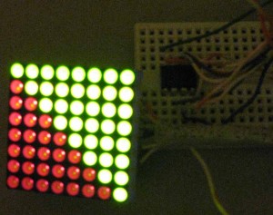
(Some pictures above… The soldered board, and also a test pattern – I could make a happy face, but davr already did so what’s the point? ;) The red LEDs are only on due to bleeding as the line is visible as the data is being shifted. This would be avoided if I were using 6 I/O pins and using LATCH as intended, but using the attiny85, I only have 5 practical I/O pins)
Overall, it was a pretty entertaining project, though I probably won’t do much further with it. It was very much a spur of the moment project, so I didn’t really have any deep plans. While I could chain many of these together I would start to have serious problems supplying the power easily, as the estimated maximum of 400mA per board is actually a significant amount of power – my present lab equipment doesn’t include a proper power supply, so maybe a future project will be to build some higher power 3.3V power supplies :)
Some Theory – A closer look at the details
(For those of you who aren’t deeply familiar with this stuff, which might be most of you.)
This matrix is an 8×8 array of bicolor Red/Green LEDs; to make it easier to deal with, instead of just giving you pins for each LED, they give you buses; In this case they connect the Anodes (positive terminals) of each row and give you one pin per row-anode-bus. Then they also connect the red and green Cathodes (independently) to column buses, and expose those buses. You can’t tell this sort of system to “hold” a specific image, it’s designed for you to only draw one row at a time – however, due to Persistence of Vision effects, you can quickly alternate between driving each row with a different pattern, and it will appear that the entire matrix is on at once. The points behind this are signal management and cost… This module gives you 8 pins for common row anodes, 8 pins for common red cathodes, and 8 pins for common green cathodes – a total of 24 pins. Actually wiring each LED independently would give you 64 LEDs * 3 pins per LED = 192 pins… Not nearly as easy to connect; and most sane designers would just connect the rows and columns together in a logical fashion on the PCB. Driving each LED independently is arguably just a bit less than 8 times as expensive as driving 8 sets of 8 LEDs and switching between them (even before you consider the PCB routing logistics to drive each LED independently!) In some systems (like giant full color LED display signs, and such) it does make sense to use per-LED driver circuitry in order to be as bright as possible, and they are rather expensive due to this and other factors :)
Some logistics have to be considered in a design like this – such as, just how much current is it going to draw? Assuming the CPLD is well programmed, at most 16 individual LEDs will be on at once. The LEDs have forward voltages of about 1.7-1.9V, and this board is driving them at 3.3V in series with 50 Ohm current limiting resistors. Walking through the power calculation, I’ll assume the LED has a 2.0V forward voltage drop (which is a worst case estimate), so the resistor will drop 1.3V when the LED circuit is switched on (as 2.0V + 1.3V = 3.3V); and as the voltage across the resistor is 1.3V, the current through the resistor (and as such, through the LED) will be 26mA (V = IR, or I = V/R, where V=1.3V, and R=50Ohm) – the reality is a little bit more complicated because LED voltage drops vary, and the CPLD will only allow so much current.
The CPLD needs to also turn individual rows on and off – but it can’t actually switch very much current on it’s own. As such, this design uses a FET that does the electrical heavy work, and the CPLD tells the FET to turn on and off. So how much current might a row take if it’s turned on? Assuming a worst case current of about 25mA per LED, the system will use 400mA if all 16 LEDs are on at once! (The CPLD by itself can only practically switch 20-30mA) I found a capable FET to handle this load though (Digikey part number DMP2004KDICT-ND) – which is a P-Channel FET capable of switching 600mA. All FETs essentially switch current flow on and off based on the voltage between the Gate and Source pins, but being a P-Channel FET means that the Source pin should be the highest voltage of the three, and it will switch on (“connect” the Source pin to the Drain pin) when the Gate’s voltage is less than the Source pin voltage by a certain amount. This FET has a switching voltage of 1V, so it’s “off” when the Gate voltage is > 2.3V, and “on” when the Gate voltage is < 2.3V – as such a logic low applied to the Gate pin turns the FET on.
Final note: A lot of these technical details are pretty shallow explanations; Things really do work this way, but there be dragons and missed details in all of the numbers I’ve given; here’s a small list of examples: The CPLD driving voltage actually depends on current, so it won’t be quite 3.3V – my example is a worst case estimate. You can see these pin driving traces sometimes in CPLD datasheets (And other times they’re linked: Xilinx FPGA/CPLD I/V Curves, see page 6 for XC9500XL family. Also, see Page 13 of the CPLD I/O User Guide for more information on I/V curves). The FETs, too, add a resistance to the load passing through them (about 0.9 ohm in this case – this is shown on the Digikey page as “Rds On”, and will also be specified in the part datasheets), so that further reduces the 3.3V that I was assuming. On a completely different tangent, FETs are capable of a lot more than just turning on and off, though they are in fact really good just for switching on/off, which is why they’re used so extensively in modern electronics (CMOS digital logic is typically almost all FETs). If you want a good book that explains all the minute details for discrete circuit design, I highly recommend The Art of Electronics- It’s a little bit older, but presents most of the important concepts in electronics very clearly and in an easily approachable way.
(It’s over! Phew- that was long. Now I’m thinking about what to write about for next week… I have a good idea for next week, but beyond that it’s a bit hazy… I have literally piles of projects around here, the problem is almost none of them are done… Perhaps this will be an incentive to work harder! That can only be a good thing, right?)
RSS feed for comments on this post. | TrackBack URI


February 4th, 2012 at 6:41 am
Hi,
My name is Pawel and Iv been into electronics for about 18 years now. I use fiber glass prototype boards but would like to start etching and designing my own. I really like your video and would like to ask you what software do you recommend to learn on?? and what is the one you are using.
Thanx Pawel C.
February 25th, 2018 at 9:37 pm
Nice project! Did you publish the source code for your CPLD design?
February 26th, 2018 at 1:12 am
I had not, but now that you have asked, I have: https://github.com/sgstair/ledmatrix_8x8redgreen
February 26th, 2018 at 5:02 pm
Many thanks!