Progress! At long last!
Over the past month I have been designing a CNC controller for various small projects I’ve been kicking around (oh things like 3d printing, building a pick&place, and some other random thoughts)
Being the hopelessly stubborn sort that I am, I decided to build it from scratch. The design work for something like this is something I enjoy immensely, and while I don’t always get everything right the first time (There are a few inefficiencies, but nothing terrible), it’s been a lot of fun and a good learning experience.
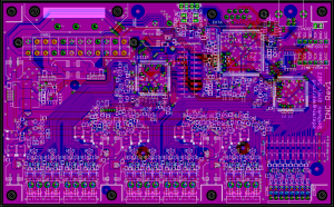
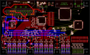
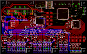
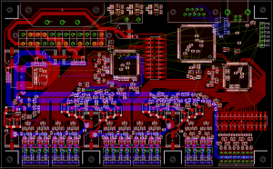
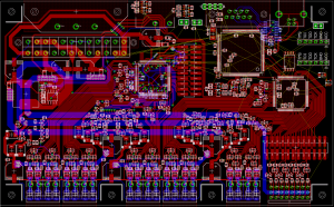
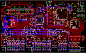
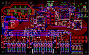
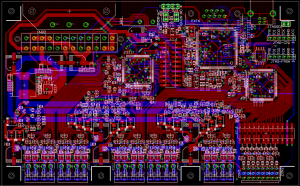
Here’s an image of the final board design, and past the break is a very long thread of text and images showing the steps getting to this point:
(After weeks of looking at this really closely, it seems amazing to me how small the board actually is)
Let’s start with the big questions:
Why design a stepper motor controller when so many already exist?
Mainly because I hadn’t done so before, and it seemed like a fun idea. Also because I have the unhealthy tendency to reinvent the wheel, and I’m not about to do anything to fix that. ;) Additionally though, I wanted to make something better than just the standard off-the-shelf motor controller
What are the design goals for this project?
The core design goal is to be very flexible. This system is rather overkill as a result, it can drive 12V and 5V steppers, and also has a lower current variable voltage rail intended to drive voltages between 5V and 12V. There is an ARM microcontroller that handles all the interface and data management, and it’s attached to two FPGAs which will be able to drive the steppers with very precise timings. As it stands, the board is designed to drive 5 stepper motors and additionally a bank of 8 standard R/C servos for miscellaneous other stuff; And each of the stepper interfaces could be used to drive two normal motors too, or resistive elements for heating, or …
Being easy to repurpose and reuse with other systems was a priority too; This design uses motor connectors which should be compatible with the system makerbot is using. For everything else (end stops, etc) it’s using 2 and 4 pin 1mm pitch JST-SH connectors which are also pretty common. There are two I2C busses which are designed to accept arbitrary sensors or controllers to be added to the system
Will you sell them / release design files / etc?
Likely one or more of the above, but I want to get it working first.
I’ll be happy to field other questions, let me know if you have any!
About design challenges:
This board started with the basic stepper motor design, and in trying to make it as useful as possible – I wound up with a motor controller as a train of 4 H-Bridges, attached to a local per-motor power rail. Each h-bridge would get two control lines from the FPGA (drive up/down), and one sense line, which tells the FPGA whether the voltage is above about 1V or so. Not a lot of information but will probably come in handy.
Ultimately this area is where the design flaw in this first revision is – The output stage of the H-Bridge is driven by a pair of FETs, a P-Fet to pull up, and an N-Fet to pull down. Since the P-Fet’s gate needs to be near the high level (these P-fets will turn on when the voltage is less than the high voltage minus a volt or so), I’m using a second stage of fets to invert the FPGA signal and make sure it can fully be turned off. I am driving the N-Fet’s gate directly with the FPGA though, and while the 3.3V signal is high enough to turn on the FET, it’s not high enough to turn it “all the way” on, so it operates in a less efficient mode. This effectively limits the amount of current I can drive efficiently to about 1A instead of 2A or so which I was designing for – but that’s not a major loss for my application so I’m going ahead with this revision anyway. I’ve found some level shifter chips that will use in subsequent versions which will solve this problem for me though, and drive both P and N FETs fully.
Routing this board was also a fun challenge, I tried to keep as many of the signals as possible on the top layer to have good return paths to ground. Ultimately this didn’t work out to be perfect, but it’s pretty good. The motor area in particular is very clean on the back side, and only has the ground plane and local power traces.
In order to make the input section as dense as possible, there are actually two PCB levels. There’s a second PCB which will stack on top of the first one, attached with one rectangular board-board connector mating, and another one with ribbon cables; This makes it possible to also enclude end-stops, rotary encoder inputs (which may not be really interesting, but may be used for something else entirely) and LEDs per motor. It’s also used for the I2C connections.
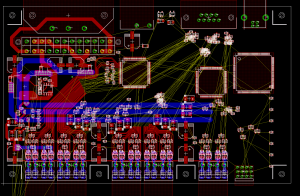
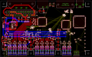
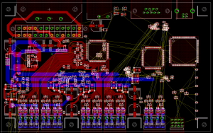
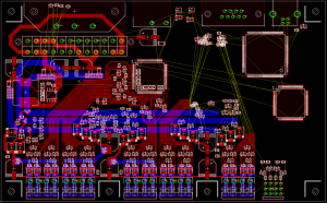
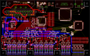
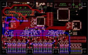
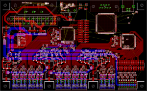
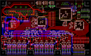
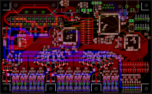
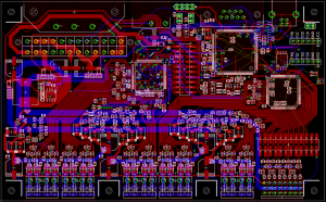
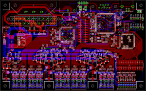
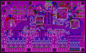
As is my custom, I have taken screenshots of the board’s layout at various arbitrary points in the design process, and the result is that you can see how the board has evolved over time.
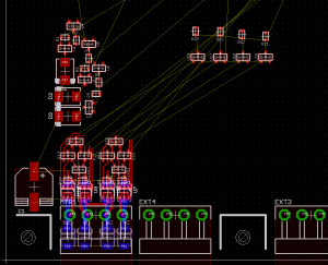
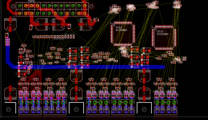
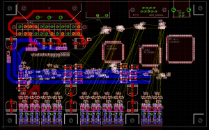
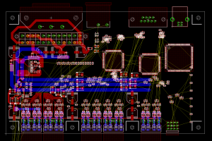
This project has been extremely long running, as far as projects go, so I have accumulated a massive 27 WIP images. They are here below with inline commentary for your amusement:
First things first – Settled on a core design and layout, and the set of parts to use. This greatly shaped what the rest of the board ended up looking like
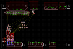
Added some more important things: Power and interface. The line voltage footprint was added for spacing reasons, and because I am considering building a line voltage -> ATX module to fit on top at some point. But that’s a crazy project in its own right.
Duplicated the motor tile for all 5 motors… And ended up with a huge mess of components!
Mostly sorted out the motor tiles at this point, and added FPGAs
The power distribution traces have been added. These are >100 mil traces for high current capacity (And the PCB will be 2Oz copper); Oh also added an ARM
Added the switching power supply for the variable voltage rail, and started working on layout for the per-motor power distribution on the first two tiles. Added 4 R/C servo outputs (was planning on putting the other 4 on the stacked second layer board)
Decided how the motor tiles should connect to the FPGA, for the first 3 tiles. Started working on routing them, and further layout/routing on the motor3-4 tiles.
Further progress routing attachments to the FPGA
More traces!
Yet more traces! Started thinking about second FPGA placement, and R/C servo connector layout
Many things here! Decided on a scheme for attaching I/O to the upper level I/O board, Also decided to put all 8 R/C servo interfaces on the bottom level to be consistent (after realizing that the top board would need to stick forward, so the JST connectors will be remotely close to the front of the other pins). And also designed the voltage/current measuring circuts, whose components were stuffed up in the top middle for now.
Started routing the power enable lines from the motor2-3 tiles, this was a bit tricky as there’s no good place to put the traces except on the back side. With the other constraints in place there really isn’t another good place to put them.
Starting to route the second FPGA, messed with a ground plane up by the switching power supply.
Routed almost all the rest of the second FPGA!
Added FPGA jtag connector, started to organize current measuring components, and attached the FPGA2 to the uC in a convenient location
Added serial level shifter, and finished organizing the current measuring components – Starting their layout.
Added a serial flash and a second JTAG connector for the ARM. This isn’t a standard ARM jtag connector, but I didn’t have space for one, this will work well enough though.
Added components for a “shutdown” switch. Decided to add a 3.3V serial connection broken out to a header, and continued stuffing the power measurement components into the space near the CPU.
Started routing power for the first FPGA. There are 3 voltage levels to manage; GND, 3.3V, and 1.2V. Routing strategy was to run 1.2V on the top layer, 3.3V in the middle on the bottom layer, and GND will fill everything else. ARM cpu is similar, except 1.8V rather than 1.2V
Finished placing and routing (most of) the power measurement components! Also finished layout of the shutdown / serial header components in the middle of the top.
Starting to route some other stuff around, and power for the ARM
Finished JTAG signals
Finished ARM chip power routing!
Now finished second FPGA power too! So very close now :)
Went back and enabled the Names layer and repositioned all of the uncooperative part labels :)
Added ground fill. Added lots of vias, started vetting design for bad features in the ground fill & vias too close to pads & etc.
Add pick&place markers, some silkscreen, further vetting, overall is pretty much done at this point!
That’s the last image I have – I have made a few tiny changes since that (found some more vias too close to pads on the back layer)
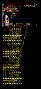
And after this board was done, I went on to build the I/O board that will sit on top of it. That was far less difficult and the images I have are below:
I’ve had fun building this board but I’m rather glad this phase is over. I’m now sending the design to be produced and will have to order a large pile of parts to populate some boards with :)
Wish me luck!
RSS feed for comments on this post. | TrackBack URI



February 27th, 2011 at 3:53 am
Awesome project, Stephen! I never knew you were interested in hardware and embedded design :). This rocks!
February 28th, 2011 at 2:44 am
Hi! Thanks :)
Yes, how much I talk about my projects definitely varies a lot over time. Hardware / embedded development is a persistent interest of mine though, and I have a lot of things underway. You’re welcome to bug me about it if you like!
May 12th, 2011 at 7:57 am
hey, did u gave up on the dstunnel project ?
October 4th, 2011 at 4:37 am
design looks very good:) would have a few questions to me if you can split the time.
I wonder if the communication between the program and the CNC control card.
That is what the task at work in the CNC control unit?
How does the program from a command?
In the form of the G-code?
Is the program undertakes all the work?
How does knowledge of the servo speed and acceleration?
specifically, about the functioning of the card, the flow diagram, please share with us
Thank you for your assistance.
October 4th, 2011 at 12:39 pm
The board is designed to work with either USB or serial; The hardware is sufficiently flexible that the specific design could work a lot of ways – at the moment I am planning to write a gcode parser that will run on the board itself, so the host will just send gcode to the board.
There will be seperate utilities for setting up the motor mappings & knowledge of speed & etc.