3 blog posts already, amazing – though very shortly I may have to start talking about far less interesting projects, or post less frequently. This is starting to take quite a bit of time, and I’m running out of interesting things I’ve been doing. :)
So, recently I’ve started looking into ASIC design – it’s will still be quite a long time before I can practically start thinking about trying to design my own chip, however, in the meantime some chip reverse engineering has attracted my attention.
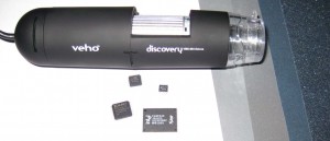
Now, I mostly operate from a home-lab environment, and it’s not really safe to involve things like… high concentrations of Nitric acid. But, having recently acquired a decent cheap USB microscope (the Veho VMS004DELUXE USB Powered Microscope), I decided to give chip disassembly a shot for the amusement value. Given my lack of professional tools this has little potential to be really educational, but it was pretty interesting. This is a pretty picture-heavy post, if that wasn’t clear enough already…
I went and found a few chips I had around, and got some sandpaper; For this test I just used 220, 600, 1500, and 2500 grit sandpaper; I had a few others around but these worked pretty well. The microscope is pretty nice, and has essentially two zoom settings, at around 20x and around 400x (or so is claimed). As such, a lot of the “chip-size” images are taken at the 20x level, and then I have zoomed in to the 400x level, taken sets of images, and stitched them together for full die images. Die images were stitched together using Microsoft ICE, a free tool that does stuff like that, it has worked pretty well for me here.
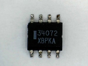
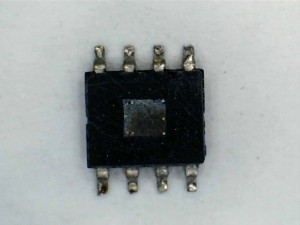
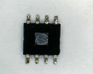
The first of the chips was some chip I had desoldered from a board I had around a very long time ago; I had no idea what it was, but it appears to be a MC34072 dual op-amp
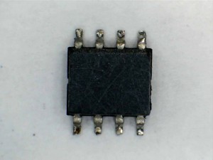
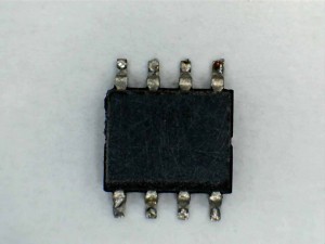
On with the sandpaper; It takes a bit of time to sand down to the die layer, so patience is important here.
I didn’t see any of the bond wires in this chip, possibly because I wasn’t sure what to be looking for. They aren’t obvious in these pictures either, I’m not sure why. After much sanding though I could see the die
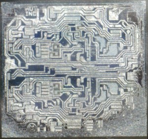
I took a full set of images at the higher magnification level at this point, though it’s pretty clear the chip packaging material is still covering a lot of the die. (this is a big image! click to zoom in!). The die is upside-down in the chip orientation I chose, so I’ve rotated the die images.
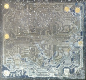
That’s pretty neat, though I’ve taken a little bit of the corner of the die off already. I spent a bit more time sanding with high grit (1500) to try to clean up the rest of the die- and while I lost some of the corners I’ve made the rest of the die a lot more visible.
That one is pretty easy to follow, it’s a very big process as it was designed apparently a long time ago (I wonder if the “72″ is the year the design was created). Unfortunately none of the other chips in this set are quite so nice :)
Also, even though you can very clearly see the metal traces in this die, what you don’t really see are the doped regions of the silicon underneath, so it’s difficult at best to infer the transistors being used. In some regions it’s possible to tell that something is different underneath (see some areas where the blue changes to dark gray), but I’m not sure what to infer from that (possibly that is material being used for resistors).
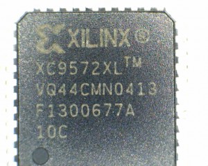
The next chip I set out to decap is one of my favorites, the Xilinx XC9572XL CPLD:
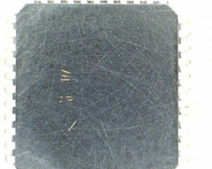
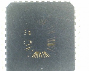
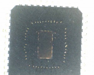
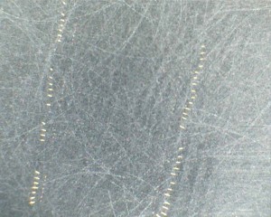
Bond wires! They actually serve as a reasonably good guide to know how well you are aligned with the die, and what areas you need to sand further so the die is more parallel to your sanded surface.
You can see that my alignment has improved but isn’t perfect yet; Also at this point I took a closer look at the bond wires (at 400x)
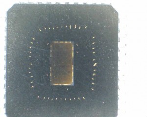
Can’t see the die at all yet, just the bond wires and packaging material. Continuing to sand…
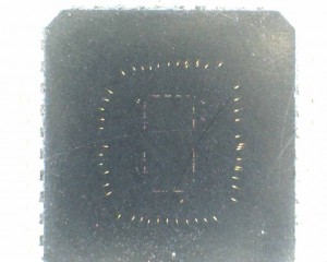
Getting closer and starting to see the die…
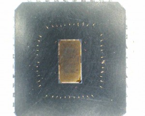
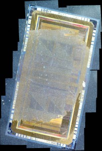
And finally breaking through the filler material to exposing the actual die surface! I then sanded a bit further with really high grit and took a few sets of images for the full die image. Ultimately I wound up using a slightly rotated orientation for taking pictures of this die, as I noticed the LED illumination at that angle made it easier to see many of the details. This method is far from perfect though – there’s still a lot of filler on the die which is only partly transparent, but I didn’t want to sand the edges away (also, too lazy now.).
Partly due to the microscope’s cheap optics and camera, and also due to the material remaining on the die, it’s very hard to discern details at this level, but you can see the larger elements in use and how they are generally connected together.
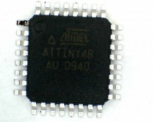
And now a very cheap AVR Chip I had around, this is an ATTiny48:
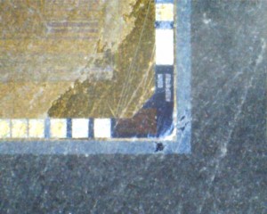
I got down to the die level without too much trouble, though I exposed one corner a lot earlier than the rest of it. After looking at that one corner closer, I decided it was important to take more of the filler material off
After taking more material off I do have a much clearer view of the die but managed to badly mess up the one corner. I did get a (mostly) complete die image – there’s a black area I somehow managed to miss :)
It’s a pretty small process, but you can generally identify the regions and their purposes. I’m not an expert on this stuff yet, but my current assumption is the shiny stuff in the bottom center is flash, the nice structured grid in the upper middle of the chip is sram, and most of the stuff above/around it is the uC logic (But I may be completely incorrect, I can see other possible interpretations.)
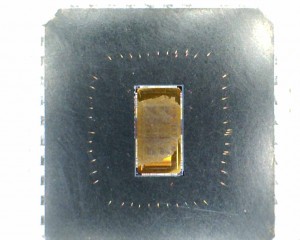
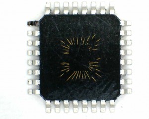
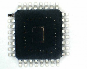
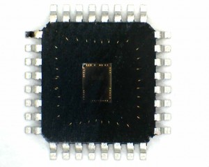
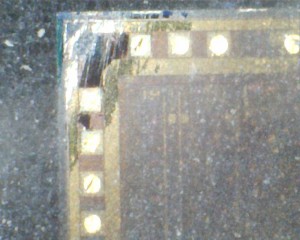
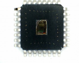
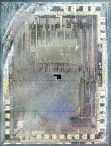
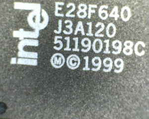
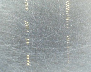
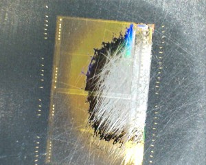
That leaves one more chip… This chip was ill fated in many ways; first it’s a bit too big for me to be able to move the microscope around above it well – but I was a bit less than patient with decapping it, and managed to seriously scratch up the die. The die showed up earlier than I thought it would, but I’ll let the images tell the story:
Oops. I cleaned up the remaining die a bit and tried to get some decent pictures, but this chip is on a much smaller process than the others and I couldn’t see much of anything that was big enough to see the structure of.
Overall this has been a pretty entertaining project for me. I think I will definitely have to try this using an acid rather than sandpaper some time in the future, and I’m already looking at better microscopes for when I get more serious with this.
In the meantime though, I hope you’ve found this as interesting as I have – thanks for reading!
Tune in next week for… Something obviously less awesome :)
RSS feed for comments on this post. | TrackBack URI
June 6th, 2010 at 12:06 am
[...] As promised, this week’s project entry is much less entertaining; [...]