Remember the PCI card from a few weeks ago?
Not too long after that, I did send out an order to manufacture some boards – and this last week they finally arrived! I’ve assembled a few, tested them, run into a few problems, solved them, and finally got a pretty basic PCI Port-80h debug card working.
In this post I’ll walk through these things, and talk some more about the PCI interface.
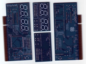
So; Early this week I received a package from MyroPCB – A cheap outsourced PCB manufacturer; I’m rather happy with the quality of these boards – it’s a reasonably simple design to produce these days I suppose, but it is still pretty neat.
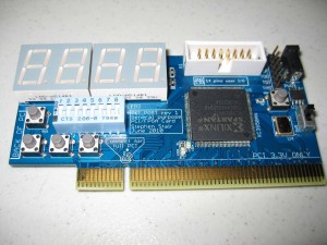
It takes some time to assemble this PCB, due to all the parts; The most annoying parts have been ones with pads strongly attached to the ground fill; Those pads have thermals seperating them from the fill, so they are not completely embedded in copper, but they’re still too well connected, and very troublesome to solder as all the heat is sucked away by the large mass of copper. Also the capacitors take some time to solder just by virtue of there being a large number of them. (And also that a large number of them have one pad attached too well to the ground fill)
At this point I didn’t do much else with this project until today;
Unfortunately, I had made a serious miscalculation – Note that the PCI edge connector on this card is 3.3V only… Now, I had built this card not long after seeing a PCI 3.3V only slot in a server system; so I made the assumption this would work great for me. In fact the PCI 3.0 specification (released in 1994!) no longer even includes the 5V PCI card slot
So that means it’s gone, right?
Well, No.
And, in fact my assumption proved to be wrong in the most incredible sense; There are literally no desktop-class motherboards on the market with 3.3V PCI slots! I spent an hour or two looking through motherboards on Newegg, and the cheapest motherboard I could find with 3.3V PCI slots was $200. (And, only had 3.3V PCI slots by virtue of them being part of 3.3V PCI-X slots)
All was not lost though, first, this board was also built to be general purpose - so it will have other uses. Also, as it turns out, it isn’t impossible to use it in modern 5V PCI slots.
Apparently, system board manufacturers don’t want to sacrifice compatibility – so while modern PCI busses are all driven with 3.3V signals, they are still using the 5V connectors and maintaining 5V compatibility – This is really annoying for my project, because my FPGA isn’t 5V tolerant like their bus controllers are, but I can work on a 3.3V bus just fine. So, to actually be able to test, I have cut out the second key slot in the PCI connector and broken the VCCIO traces that would otherwise connect 5V to my 3.3V rail in the 5V slot. The PCI connector has a bundle of different voltage rails – but in a 3.3V-only card, like I made, the I/O voltage levels are intended to be connected to the 3.3V rail – so I did connect them – Unfortunately, being compatible with a 5V slot means those I/O voltage levels are 5V. It’s not ideal to just disconnect them, as they are supposed to have bypass capacitors in order to reduce noise, but I didn’t have many options with this, so I have just disconnected my card from the I/O voltages completely.
With this modification, my card is quite happy to work in the motherboards I have around – The caveat is, since my FPGA isn’t 5V tolerant, if I put it in with a 5V device (which does typically drive the bus up to 5V), it will likely damage my device. However, for what I’d like to do, I can live with this, and I can redesign the board if I ever actually need 5V tolerance.
After resolving how to test my board as a PCI device, I set out to write a first simple test firmware, to verify that the core functionality worked- This just drives the display and sets the LED values based on the switches present on the system.
It was at this point that I noticed the green “programming done” LED had accidentally been populated with a red LED on this board – oops. I will have to go back and fix that later.
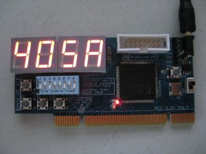
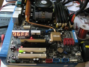
A few short steps further, and I converted the test program to firmware for watching the port 80h I/O Writes on the PCI bus – I had an old motherboard around from a system upgrade some time ago, connected it up, and it does appear to be working! After powering up the system, the display cycled through a number of values exactly the way it should; In the image below you can see the last 2 values it observed written to port 80h.
So,A few short notes about PCI devices – First, this isn’t actually a full PCI device; It does not interfere with the bus any more than is necessary to make electrical contact- it is only listening to the bus in order to see this information (as such it’s out of spec). It is actually possible to make a full PCI device with this card, and that’s on my list of things to do eventually as well.
The PCI bus though, is essentially a collection of signals – there are 32 address/data lines, and a number of control signals; At its core though are the PCI Clock signal, a FRAME signal (each transaction on the bus is a frame), the 32 address/data lines, 4 lines which are used as both a control word, and as 4 individual byte enables (to enable byte granularity in the 32bit value) – Beyond these are some handshaking signals (IRDY/TRDY), sanity checking (Parity), error reporting (PERR/SERR), transaction abort (STOP), System reset (RST), and location-based device identification (IDSEL/DEVSEL)
In order to listen for a specific port write on the bus though, you only really need the CLK, FRAME, data lines, and the 4-bit control word / byte enable – All PCI signals are sampled on a rising clock edge, the controller starts a frame by asserting FRAME on a clock edge. When it does this, it also sets the 4-bit control word to the transaction type, and for some types of transactions also sets the address lines to the related address.
What my card is doing, is waiting for reset to finish; then every frame that starts, it checks if it is an I/O write with address = 0×00000080; If so, it listens on the next cycle, and if byte enable 0 is set, it will accept the data in the bottom 8 bits of the data lines as a new port 80h write – In any case, it waits for the frame to finish, and then continues waiting for another frame to start.
Sounds simple? It really is.
Making a real PCI device though will be a lot more challenging, and I’ll be sure to document that when I get around to it :)
Small update: I should probably also mention the significance of Port 80h – System BIOS manufacturers have standardized on using port 80h as a debug port of sorts, they write a byte to that port to indicate which section of the BIOS code is running; As such, there are a number of cheaply available “PC Diagnostic” boards, which do essentially what I’m doing here, just listen for Port 80h accesses and display the values. The capability to see this code is helpful when diagnosing a difficult motherboard problem, to be sure… but it’s also helpful when writing and debugging low-level code when little else on the system is running, as you can add writes to 80h that give you information about what stage of execution your program is in.
RSS feed for comments on this post. | TrackBack URI


