The road to 3D Printing, part 4
Armed with a blinking LED program, I set to work attempting to flesh out the rest of the software for the CNC board. I built and tested a nested vectored interrupt handler, and started trying to port my USB stack from another chip that has very similar USB hardware. As time went on though, the outlook became a bit bleak; A number of things did not appear to be working as intended on this chip, and the manufacturer’s example code included bizzare comments and workarounds for some pretty impactful bugs that weren’t otherwise documented. Not confident that I would be able to make this chip work the way that I wanted, and being less than thrilled with the ease of assembly and some of the design of the CNC Rev1 board, I decided to make a new CNC board.
My design goals would be:
- Ensure the design will work, by using chips I’m familiar with & already have code working on.
- Reduce complexity by only having one motor driving voltage, but still allow that voltage to be changed.
- Reduce the part count per motor, by consolidating components into fewer packages and taking a different design path driving the motors.
As usual, I have a progression of design image captured through the process to give an idea of how the project unfolded:

1) Decided on the core pieces to use, and approximate board size. CNC rev 2 is based around a single BGA FPGA, and an ARM Cortex-M3 chip I use heavily in other projects (LPC134x). The plan at this point was to drive 6 motors and allow USB from both the micro and from the FPGA (to eventually produce a working system without the micro)

2) Prototyping the component placement for a single motor block. Changes from CNC Rev1 are: Clamp diodes are now more integrated (rotated chip replaces 4 diodes that were on the other side of the board), using a level shifter chip rather than an arrangement of fets (each level shifter replaces 6 fets & a dozen resistors)

3) Decided 6 was too many, dropped back to 5 motor blocks; Added header block for end-stop switches, and resistors / clamp diodes to feed back motor pins to the FPGA safely.

4) Routed the power trace for motor voltage; The header at the top allows the motor voltage to be changed by an expansion board, or the pins can just be jumpered to provide the 12V default.

5) Adding more support parts and starting to make some connections within the motor blocks and for the microcontroller.

6) Adding some more external connectivity; the 4-pin JST 2mm connectors are for external I2C connections, and there’s a 4×3 pin header that can be used to drive servos.

7) Prototyping the motor block connections

8) Adding yet more important stuff! The big header was only added temporarily though, to provide a linear target to attach pins to (to easily see that the motor block signals came out in a specific order)

9) Added analog current measurement stuff. I drop the FPGA’s USB port as I note space and pins are likely to be an issue, and I don’t really want to drop the uC anymore because it’s an easy way to get ADC results.

10) After much planning, have decided on the FPGA orientation and started to map the pins to the fpga.

11) Finished mapping the motor blocks to the FPGA, and generally organized the analog stuff into a nice cranny up by the ATX connector.

12) Showing the breakout of fpga signals so far. I opted to allow using a much cheaper FPGA so not all of the pins are present/connected. In order to remedy this sometimes I run internal pins out through some of the (unconnected) outer pins. (I need all the I/O I can get!)

13) Starting to route the motor blocks to the FPGA. When the planning is done this is generally pretty simple.

14) Continuing that…

15) All motor blocks connected!

16) Started to route peripherals on the right side, and worked on organizing the remainder of the components to fit in available space.

17) Finished routing all the right-side signals! So far all the routed signals are all on one layer, pretty happy about that. There are around 90 signals connected to the FPGA at this point.

18) My attention turns to the microcontroller which is now almost fully routed, and I start routing 3v3 power and FPGA jtag.

19) FPGA Power. Srs bzness. the really thin traces are gnd, and are only there to keep track of connected things, there will be a gnd fill later. Ultimately this is not going to be a very demanding application for the FPGA, the pins will not be switching at a high frequency.

20) With almost everything else done, attention turns to finishing the power routing for the level shifters on the motor blocks.

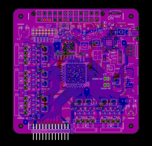
21) That is finished and ground fill is added. This is the electrically complete board.

22) Even that was not entirely complete… Also the component names needed to be adjusted to ensure they are readable. This is effectively the final board.
I have another bigger version of this image up on flickr:
Do be sure to point out any flaws ;)
I expect to get the first copies of this board back today (maybe) – I sent this board off in Laen’s order to get prototypes back relatively cheaply in case there are bugs, but if there aren’t problems I will probably manufacture a few dozen more.
So now the blog entries on this reach the current point in time, and I have to do actual work to write more of this path – wish me luck :)
(Will be continued in part 5)
RSS feed for comments on this post. | TrackBack URI
March 8th, 2012 at 2:18 am
Are you going to do a microstepping and SD-card interface?
3d printing of big parts takes a loooong time so autonomous printing is really usefull :))
You can look at my project at github:
https://github.com/sevikkk/VP2motion
It’s fpga based motion controller for my reprap-like 3d printer.
I’m using .s3g files for makerbot printers as intermediate format. I do simple acceleration in hardware and path planning and synchronized acceleration profiles in postprocessor after slicing.
March 11th, 2012 at 11:31 pm
Not yet sure if I’m going to implement microstepping; but it’s a possibility. I’ve so far been just trying to get the core functionality put together (which, now, it pretty much is)
I will probably experiment with making it autonomous at some point, there’s an onboard SPI flash that has a lot of space free; however the board was designed to be a good friend to a PC :)
Nice setup (https://picasaweb.google.com/114257244810512271993/3dMf70#5713208861615163394) – I like the SD card interface :P
My fpga is I think a few orders of magnitude smaller than yours though – it’s currently implementing a minimal (pure vhdl) motor control queue, so all the acceleration/etc is to be done in the host currently. I am planning to switch to a bigger FPGA though, and will consider a more complicated hardware implementation then.